- 您现在的位置:买卖IC网 > Sheet目录518 > SQJ941EP-T1-GE3 (Vishay Siliconix)MOSFET DUAL P-CH 30V PPAK 8SOIC
�� �
�
�SQJ941EP�
�www.vishay.com�
�Vishay� Siliconix�
�Automotive� Dual� P-Channel� 30� V� (D-S)� 175� °C� MOSFET�
�PRODUCT� SUMMARY�
�V� DS� (V)�
�R� DS(on)� (� ?� )� at� V� GS� =� -� 10� V�
�R� DS(on)� (� ?� )� at� V� GS� =� -� 4.5� V�
�I� D� (A)� per� leg�
�Configuration�
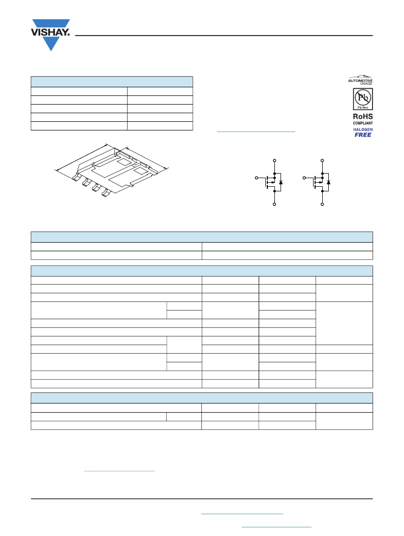
�PowerPAK� ?� SO-8L� Dual�
�-� 30�
�0.024�
�0.039�
�-8�
�Dual�
�FEATURES�
�?� TrenchFET� ?� Power� MOSFET�
�?� 100� %� R� g� and� UIS� Tested�
�?� AEC-Q101� Qualified� d�
�?� Material� categorization:� ?�
�For� definitions� of� compliance� please� see�
�www.vishay.com/doc?99912�
�?�
�5m�
�3m�
�6.1�
�m�
�5.1�
�m�
�S� 1�
�S� 2�
�D�
�2�
�D�
�1�
�G� 1�
�G� 2�
�4�
�G� 2�
�S� 2�
�3�
�2�
�G� 1�
�1�
�S� 1�
�Bottom� View�
�ORDERING� INFORMATION�
�D� 1�
�P-Channel� MOSFET�
�D� 2�
�P-Channel� MOSFET�
�Package�
�Lead� (Pb)-free� and� Halogen-free�
�ABSOLUTE� MAXIMUM� RATINGS� (T� C� =� 25� °C,� unless� otherwise� noted)�
�PowerPAK� SO-8L�
�SQJ941EP-T1-GE3�
�PARAMETER�
�Drain-Source� Voltage�
�Gate-Source� Voltage�
�SYMBOL�
�V� DS�
�V� GS�
�LIMIT�
�-� 30�
�±� 20�
�UNIT�
�V�
�Continuous� Drain� Current� a�
�T� C� =� 25� °C�
�T� C� =� 125� °C�
�I� D�
�-8�
�-8�
�Continuous� Source� Current� (Diode�
�Pulsed� Drain� Current� b�
�Single� Pulse� Avalanche� Current�
�Single� Pulse� Avalanche� Energy�
�Maximum� Power� Dissipation� b�
�Conduction)� a�
�L� =� 0.1� mH�
�T� C� =� 25� °C�
�T� C� =� 125� °C�
�I� S�
�I� DM�
�I� AS�
�E� AS�
�P� D�
�-8�
�-� 32�
�-� 24�
�28.8�
�55�
�18.5�
�A�
�mJ�
�W�
�Operating� Junction� and� Storage� Temperature� Range�
�Soldering� Recommendations� (Peak� Temperature)� e,� f�
�T� J� ,� T� stg�
�-� 55� to� +� 175�
�260�
�°C�
�THERMAL� RESISTANCE� RATINGS�
�PARAMETER�
�SYMBOL�
�LIMIT�
�UNIT�
�Junction-to-Ambient�
�Junction-to-Case� (Drain)�
�PCB� Mount� c�
�R� thJA�
�R� thJC�
�85�
�2.7�
�°C/W�
�Notes�
�a.� Package� limited.�
�b.� Pulse� test;� pulse� width� ?� 300� μs,� duty� cycle� ?� 2� %.�
�c.� When� mounted� on� 1"� square� PCB� (FR4� material).�
�d.� Parametric� verification� ongoing.�
�e.� See� solder� profile� (� www.vishay.com/doc?73257� ).� The� PowerPAK� SO-8L.� The� end� of� the� lead� terminal� is� exposed� copper� (not� plated)� as� a�
�result� of� the� singulation� process� in� manufacturing.� A� solder� fillet� at� the� exposed� copper� tip� cannot� be� guaranteed� and� is� not� required� to�
�ensure� adequate� bottom� side� solder� interconnection.�
�f.� Rework� conditions:� manual� soldering� with� a� soldering� iron� is� not� recommended� for� leadless� components.�
�S12-1848-Rev.� C,� 30-Jul-12�
�1�
�Document� Number:� 65546�
�For� technical� questions,� contact:� automostechsupport@vishay.com�
�THIS� DOCUMENT� IS� SUBJECT� TO� CHANGE� WITHOUT� NOTICE.� THE� PRODUCTS� DESCRIBED� HEREIN� AND� THIS� DOCUMENT�
�ARE� SUBJECT� TO� SPECIFIC� DISCLAIMERS,� SET� FORTH� AT� www.vishay.com/doc?91000�
�发布紧急采购,3分钟左右您将得到回复。
相关PDF资料
SQJ964EP-T1-GE3
MOSFET DUAL N-CH 60V PPAK 8SOIC
SQJ970EP-T1-GE3
MOSFET DUAL N-CH 40V PPAK 8SOIC
SQM110N04-02L-GE3
MOSFET N-CH D-S 40V TO263
SQM110N04-03L-GE3
MOSFET N-CH D-S 40V TO263
SQM110N06-04L-GE3
MOSFET N-CH D-S 60V TO263
SQM40N10-30-GE3
MOSFET N-CH D-S 100V TO263
SQM85N03-06P-GE3
MOSFET N-CH D-S 30V TO263
SQR50N03-06P-GE3
MOSFET N-CH D-S 30V TO263
相关代理商/技术参数
SQJ942EP
制造商:VISHAY 制造商全称:Vishay Siliconix 功能描述:Automotive Dual N-Channel 40 V (D-S) 175 C MOSFETs
SQJ942EP-T1-GE3
制造商:VISHAY 制造商全称:Vishay Siliconix 功能描述:Automotive Dual N-Channel 40 V (D-S) 175 C MOSFETs
SQJ951EP
制造商:VISHAY 制造商全称:Vishay Siliconix 功能描述:Automotive Dual P-Channel 30 V (D-S) 175 ?°C MOSFET
SQJ960EP
制造商:VISHAY 制造商全称:Vishay Siliconix 功能描述:Automotive Dual N-Channel 60 V (D-S) 175 ?°C MOSFET
SQJ960EP-T1-GE3
功能描述:MOSFET 60V 8A 34W RoHS:否 制造商:STMicroelectronics 晶体管极性:N-Channel 汲极/源极击穿电压:650 V 闸/源击穿电压:25 V 漏极连续电流:130 A 电阻汲极/源极 RDS(导通):0.014 Ohms 配置:Single 最大工作温度: 安装风格:Through Hole 封装 / 箱体:Max247 封装:Tube
SQJ962EP
制造商:VISHAY 制造商全称:Vishay Siliconix 功能描述:Automotive Dual N-Channel 60 V (D-S) 175 ?°C MOSFET
SQJ962EP-T1-GE3
功能描述:MOSFET 60V 8A 25W RoHS:否 制造商:STMicroelectronics 晶体管极性:N-Channel 汲极/源极击穿电压:650 V 闸/源击穿电压:25 V 漏极连续电流:130 A 电阻汲极/源极 RDS(导通):0.014 Ohms 配置:Single 最大工作温度: 安装风格:Through Hole 封装 / 箱体:Max247 封装:Tube
SQJ963EP
制造商:VISHAY 制造商全称:Vishay Siliconix 功能描述:Automotive Dual P-Channel 60 V (D-S) 175 ?°C MOSFET